

Skip to content
Company Logo
  • Home
    • Trident Techlabs Limited (India)
    • Trident Techlabs LLC FZ (UAE)
    • Techlabs Semiconductor Pvt. Ltd. (Subsidiary)
  • About Us
    • Company Overview
    • Executive Leadership
  • Solutions
    Engineering Solutions
    Power System Solutions
    Cyber Security Services & Solution
    Techlabs Semiconductor
    style="width: 100%; height: 100%; object-fit: cover;">
    Academics
    style="width: 100%; height: 100%; object-fit: cover;">
    CAE
    style="width: 100%; height: 100%; object-fit: cover;">
    EDA
    style="width: 100%; height: 100%; object-fit: cover;">
    Products
    style="width: 100%; height: 100%; object-fit: cover;">
    Services
    style="width: 100%; height: 100%; object-fit: cover;">
    style="width: 100%; height: 100%; object-fit: cover;">
    style="width: 100%; height: 100%; object-fit: cover;">
  • Investor Charter
  • Events
    • Upcoming Events
    • Past Events
  • Careers
    • About Our Work
    • Job Listings
  • Resources
    • Webinars
    • Case Study
    • Brochure
    • Blog
  • Contact
Call Anytime +91-11-61811100
  • Home
    • Trident Techlabs Limited (India)
    • Trident Techlabs LLC FZ (UAE)
    • Techlabs Semiconductor Pvt. Ltd. (Subsidiary)
  • About Us
    • Company Overview
    • Executive Leadership
  • Solutions
    • Engineering Solutions
      • Engineering Solution
      • Academics
      • CAE
      • EDA
    • Power System Solutions
      • Products and Design Tools
      • Consulting Services
    • Cyber Security Services & Solutions
    • Techlabs Semiconductor
  • Investor Charter
  • Events
    • Upcoming Events
    • Past Events
  • Careers
    • About Our Work
    • Job Listings
  • Blog
  • Contact
Custom ASIC Design Services

The Role of Power, Performance and Area in Custom ASIC Design Services

Posted on September 22, 2026September 22, 2026 by Trident Techlabs Limited

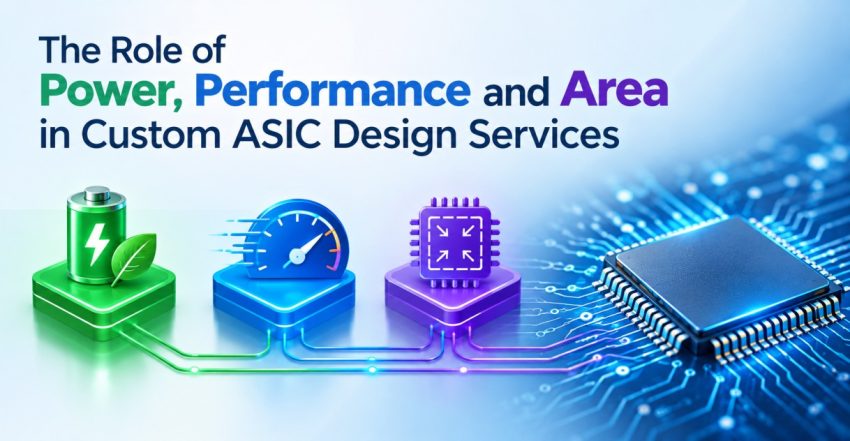
The design of a chip is not just a question of having to perform a certain function. Engineers need to also decide its speed, the amount of energy it can use and the amount of physical space it can take up. In custom ASIC design services, these three considerations are called Power, Performance and Area (PPA) and are very significant.

A successful ASIC will be one where these factors will be balanced appropriately in accordance with the needs of the product. An important consideration in the design process is that optimising one aspect can impact on another and so PPA optimisation is important.

Understanding Power

Almost every electronic device these days comes with power consumption as a factor to consider. Power usage can cause too much heat, shorter battery life and impact system reliability.

A low power usage is especially relevant in battery-powered devices like wearables, portable devices or IoT devices. Therefore, engineers involved in the custom design services for ASICs can implement methods like eliminating unnecessary switching activity, optimizing operating parameters, and developing efficient circuits.

Sometimes, power and performance go together. The aim is to have an optimized design while not sacrificing the necessary functions, by finding where energy is being used in the design.

Measuring Performance

The performance of a chip is its ability to carry out functions efficiently and speedily. This may translate to increased processing speed, reduced response time or greater number of operations in a given time.

The requirements for performance of a chip used in an artificial intelligence, networking, automotive system or high-speed communications system can be demanding. Operating frequency, data paths, memory access, and circuit architecture are just a few aspects that engineers will need to take into account when designing.

For custom ASIC design services, performance goals are set early since the architectural choices made in the initial stages of the design can have a major impact on the final chip.

Utilizing Area:Optimizing Area:

The area is the number of square millimeters of silicon needed to make the chip. The smaller design may mean that the manufacturing costs are lower, and it might fit more of the functions into a smaller package.

But area reduction isn’t all about cutting parts out. All circuits serve a purpose; too much optimization can have an impact on the performance, power usage or functionality of that circuit.

Engineers thus seek to make efficient use of silicon with the necessary capabilities. When it comes to making chips in large volume, even a slight improvement in the use of area could make a difference.

A balanced approach is essential to PPA.

Power, performance, and area are related. To get higher performance it may be necessary to add extra circuit components or to run at higher frequencies, thereby increasing power or area. Likewise, minimizing area can be problematic for some performance or energy efficiency applications.

That’s why custom ASIC design services are a never-ending process of evaluation and optimisation, rather than three distinct goals.

The correct ratio will depend on the use. The company could design a smartphone chip that takes energy efficiency into account more heavily, or design a data-processing accelerator that is more performance-focused. No universal PPA formula exists for all the ASICs.

PPA Starts With the Right Design Decisions

PPA optimisation starts well before product manufacture. The design of the architecture, logic design, memory selection, verification, physical design and implementation decisions can all affect the final result.

With careful planning, engineers can know about potential bottlenecks before they are given a chance to hamper the process, rather than when it’s too late.

Conclusion

Two key factors in today’s chip development are power and performance, and area. They affect the performance of an ASIC, its size and its effectiveness. In this way, custom ASIC design services can take into account all these considerations during the design process, ensuring the development of efficient, reliable, and optimized chips for specific applications.

Also Read: Engineering the Shield: How Vendor-Neutral Integration Eradicates Technical Debt in Defense SOCs

Leave a Reply Cancel reply

Your email address will not be published. Required fields are marked *

Send Query

    Recent Posts

    • The Role of Power, Performance and Area in Custom ASIC Design Services
    • Engineering the Shield: How Vendor-Neutral Integration Eradicates Technical Debt in Defense SOCs
    • The Art of Cyber Deception: Turning the Tables on Lateral Movement in Enterprise Networks
    • What the Data Leak in Banking Institution Teaches Organizations about Identity Security
    • The Lifecycle of Resilience: How Proactive Managed Support Keeps Public Sector SOCs Ahead of the Threat Curve

    Recent Comments

    1. The Role of Power, Performance and Area in Custom ASIC Design Services on Engineering the Shield: How Vendor-Neutral Integration Eradicates Technical Debt in Defense SOCs
    2. Engineering the Shield: How Vendor-Neutral Integration Eradicates Technical Debt in Defense SOCs on The Art of Cyber Deception: Turning the Tables on Lateral Movement in Enterprise Networks
    3. The Art of Cyber Deception: Turning the Tables on Lateral Movement in Enterprise Networks on What the Data Leak in Banking Institution Teaches Organizations about Identity Security

    Archives

    • September 2026
    • August 2026
    • July 2026
    • June 2026
    • May 2026
    • April 2026
    • March 2026
    • February 2026
    • January 2026
    • December 2025
    • November 2025
    • October 2025
    • September 2025
    • August 2025
    • July 2025
    • June 2025
    • May 2025
    • April 2025
    • March 2025
    • February 2025
    • January 2025
    • December 2024
    • November 2024
    • October 2024
    • September 2024
    • August 2024
    • July 2024
    • June 2024
    • May 2024
    • April 2024
    • March 2024
    • February 2024
    • January 2024
    • December 2023
    • November 2023
    • October 2023
    • September 2023
    • August 2023

    Categories

    • ARC Flash
    • Arc Flash Risk Assessment
    • ASIC Design and Implementation
    • CAE
    • CAM
    • Cybersecurity
    • Electric Arc
    • Electronics Engineering
    • FPGA Design and Validation
    • Mechanical Engineering
    • PCB Design
    • Power Integrity
    • Reliability Analysis
    • Safety Assessment
    • Semiconductor Solutions
    • Signal Integrity
    • software provider
    • Structural Analysis
    • Thermal Design

    Our Certificates

    • CMMI Level 3
    • Information Security Management System (ISO 27001:2022)
    • Quality Management System (ISO 9001:2015)
    • Information Technology Service Management (ISO/IEC 20000-1:2018)
    • Occupational Health & Safety Management System (ISO 45001:2018)

    Our Services

    • Engineering Solutions
    • Power System Solutions
    • Cybersecurity Solutions
    • Semiconductor Services

    Quick Links

    • Home
    • Company Overview
    • Investor Charter
    • Events
    • Blogs
    • Contact Us
    • Privacy Policy

    Trident Techlabs Limited

    • White House, 1/18-20, 2nd Floor, Rani Jhansi Road, New Delhi - 110055
    • +91-11-61811100
    • corporate@tridenttechlabs.com

    © All Copyright 2026 by Trident Techlabs

    imunify-bot-check