


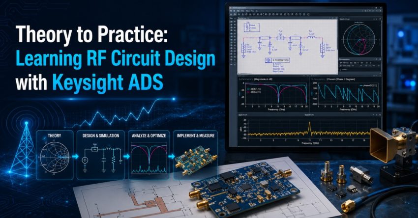
The principles of RF and microwave engineering are challenging to understand solely from theory. Even though classroom learning gives the required foundations, it is more beneficial for the students and researchers to use their knowledge in a practical environment. Keysight Advanced Design Systems closes this gap by giving an opportunity for using theoretical knowledge for creating simulations of the RF circuit designs.
Starting from the creation of the first schematic to analysis of performance and creation of the final layout, the software creates a comprehensive workflow that will help the learner understand the process of design of the RF circuit.
Moving Beyond Classroom Concepts
To learn the principles of RF circuit design, it is not enough just to know the corresponding equations and diagrams of the circuits. Engineers have to learn how the components interact, how the signals work in high frequency, and how the decisions about design affect performance of the circuit.
Keysight Advanced Design Systems gives the opportunity to understand all this in practice, creating a virtual environment for testing the behavior of circuits and evaluating the results of their behavior.
Creating Circuits Through Schematic Capture
The first step of the design process is called schematic capture. In ADS, users are capable of creating RF circuits by putting components and connecting them in order to create full-fledged circuits.
In this way, students learn how the specific component contributes to the work of the whole circuit. As they create different configurations of circuits, they become more confident in turning theoretical concepts of circuits into practice.
Understanding Performance with S-Parameter Analysis
The most critical aspect of the RF circuit design process is the evaluation of its performance. With the use of Keysight ADS, users can analyze such a critical parameter as S-parameters of the RF circuit.
This way, one can find out how the RF signals go through a certain circuit. This allows students to understand how the circuits operate. Comparing the results of simulation with the theoretical data, learners obtain new knowledge about RF and microwave engineering.
Improving Designs Through Optimization
Design is rarely created at once. It can be improved with some changes of the values of components or other circuit parameters.
With the help of Keysight ADS, learners can optimize their circuit in order to improve its parameters. In contrast to the manual search for various combinations, the program provides more advanced options, the software helps identify improved design parameters that meet the desired objectives.
This process teaches learners how engineers approach design refinement in professional RF development environments.
Completing the Workflow with Layout Design
After achieving the satisfactory and necessary simulation results, the design process continues with layout development. Keysight ADS enables the transformation of a schematic into layout to help the user understand how a circuit gets ready for implementation.
The design process including both the electrical part and layout creation gives the student a full understanding of how RF design goes.
Bridging Theory and Real-World RF Product Development
One of the best features of Keysight ADS is the possibility to combine theoretical learning with practical engineering. Students have an opportunity not only to learn concepts but also implement them through a full-fledged design cycle similar to those used in the industry.
From the schematic capture and S-parameter analysis to optimization and layout creation, each step provides practical application of theoretical knowledge. Researchers, in their turn, can quickly test new ideas and evaluate their feasibility before implementation.
Conclusion
In the Keysight Advanced Design System (ADS), students and researchers are taught the systematic way of designing circuits by simulations. In doing so, all aspects of the process from capturing the schematic to S-parameter analysis, optimization, and layout are included. Through this process, it will be possible for the learner to gain knowledge and experience.
As technology develops, especially those involving RFs and microwaves, students will be prepared to utilize simulation software through Advanced Design Systems (ADS).