

Skip to content
Company Logo
  • Home
    • Trident Techlabs Limited (India)
    • Trident Techlabs LLC FZ (UAE)
    • Techlabs Semiconductor Pvt. Ltd. (Subsidiary)
  • About Us
    • Company Overview
    • Executive Leadership
  • Solutions
    Engineering Solutions
    Power System Solutions
    Cyber Security Services & Solution
    Techlabs Semiconductor
    style="width: 100%; height: 100%; object-fit: cover;">
    Academics
    style="width: 100%; height: 100%; object-fit: cover;">
    CAE
    style="width: 100%; height: 100%; object-fit: cover;">
    EDA
    style="width: 100%; height: 100%; object-fit: cover;">
    Products
    style="width: 100%; height: 100%; object-fit: cover;">
    Services
    style="width: 100%; height: 100%; object-fit: cover;">
    style="width: 100%; height: 100%; object-fit: cover;">
    style="width: 100%; height: 100%; object-fit: cover;">
  • Investor Charter
  • Events
    • Upcoming Events
    • Past Events
  • Careers
    • About Our Work
    • Job Listings
  • Resources
    • Webinars
    • Case Study
    • Brochure
    • Blog
  • Contact
Call Anytime +91-11-61811100
  • Home
    • Trident Techlabs Limited (India)
    • Trident Techlabs LLC FZ (UAE)
    • Techlabs Semiconductor Pvt. Ltd. (Subsidiary)
  • About Us
    • Company Overview
    • Executive Leadership
  • Solutions
    • Engineering Solutions
      • Engineering Solution
      • Academics
      • CAE
      • EDA
    • Power System Solutions
      • Products and Design Tools
      • Consulting Services
    • Cyber Security Services & Solutions
    • Techlabs Semiconductor
  • Investor Charter
  • Events
    • Upcoming Events
    • Past Events
  • Careers
    • About Our Work
    • Job Listings
  • Blog
  • Contact
PCB Manufacturing Companies in India

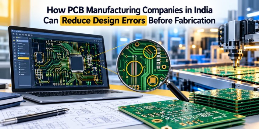
How PCB Manufacturing Companies in India Can Reduce Design Errors Before Fabrication

Posted on October 23, 2026October 23, 2026 by Trident Techlabs Limited

Design errors in a Printed Circuit Board (PCB) can cause revisions to be repeated and the development of the product to be longer and more expensive. These are some of the issues that must be identified prior to fabrication in a business developing complex electronic systems to maintain the product quality and meet the performance requirement. The structured engineering approach in PCB manufacturing companies in India is one such method, encompassing design reviews, simulation, and verification, to prevent unnecessary errors before entering production.

Perform a Thorough Design Review

The review of the PCB layout can be an essential starting point to uncover possible problems. The engineers need to verify all the components placement, routing, clearance, connections, and layering with the design requirements.

Design Rule Checks (DRC) automatically check for trace spacing, board clearances, manufacturing constraints. But the passing of DRC does not mean that a board will act correctly. If engineers do not perform further analysis, they may not be able to identify electrical performance issues.

A comparison between the schematic diagram and the PCB layout helps one to be aware of any connectivity problems before embarking on the fabrication process.

Use of Simulation to Detect Problems

By simulation of the design, one is able to analyze the design before creating the actual product. Depending on the application, various analysis methods can be used to explore the electrical performance, the thermal behavior, and electromagnetic effects.

Signal integrity analysis is of great significance for high-speed PCBs. Even when it looks like a signal’s routing is correct, impedance discontinuities and crosstalk and interrupted return paths can cause signal distortion or timing issues.

There are two types of analysis – pre-layout analysis can set appropriate design constraints and post-layout analysis can check the actual routed board. Both methods can be used to work out the potential weaknesses and enable engineers to make informed changes to the design.

Check on Component Selection and Compatibility

Problems can occur if the wrong components are chosen which will inevitably lead to difficulties after fabrication. The components need to comply with the electrical requirements, operating temperature ranges, power needs, interface requirements etc.

The availability of components as well as the lifecycle status and package compatibility should also be taken into account. When checking footprints on manufacturer datasheets, there is less risk of misinterpreting the dimensions, pin assignments or assembly related problems.

In the case of complex electronic products, compatibility between the interconnected components can be checked before functional issues arise during testing and validation.

Consider Design-for-Manufacturing Requirements

PCB design that functions electrically might not work during manufacturing or assembly due to layout design issues.

Design-for-Manufacturing (DFM) reviews are used to determine if the board can be reliably manufactured in the desired manufacturing processes. Minimal trace width and spacing, drill size and copper clearances and stack up are all important.

The communication between the design engineers and manufacturing team help in recognizing the process restrictions early in the production process. This can minimize rework and ensure uniform boards.

Include Build Verification in the Development Process

A systematic design process is needed to minimize PCB design mistakes, not one last review. Design requirements should be reviewed, automated checks should be run, and corrections checked and made appropriate before manufacturing files are released to the teams.

This process can be assisted using enginee ring solutions that include PCB analysis, simulation and design verification. Trident Techlabs offers engineering solutions, including simulation and semiconductor design, to organisations facing challenges with complex electronics development.

Conclusion

PCB manufacturing companies in India can minimize the design mistakes by using detailed layout reviews, simulation, component verification and design for manufacturing checks. Recognizing potential problems before fabrication can help to reduce the amount of rework, limit development costs and increase the confidence in product performance.

The goal is not just to create a manufacturable PCB, but to ensure that the design is electrically sound and mechanically correct and is ready to be manufactured reliably.

Frequently Asked Questions

How can PCB manufacturing companies in India reduce design errors before fabrication?

PCB manufacturing companies in India can reduce errors through design reviews, simulation, component verification, and Design-for-Manufacturing (DFM) checks.

What are the most common PCB design errors before manufacturing?

Common PCB design errors include incorrect component placement, routing mistakes, insufficient clearances, footprint mismatches, and signal integrity issues.

What is a Design Rule Check (DRC) in PCB design?

A Design Rule Check (DRC) automatically identifies PCB layout violations involving trace spacing, clearances, and manufacturing constraints.

Why is PCB simulation important before fabrication?

PCB simulation helps detect signal integrity, thermal, and electromagnetic issues before fabrication, reducing costly redesigns and performance failures.

What is the difference between DRC and DFM in PCB manufacturing?

DRC checks layout rules and constraints, while DFM evaluates whether a PCB design can be manufactured reliably.

How can signal integrity analysis prevent PCB design failures?

Signal integrity analysis identifies impedance discontinuities, crosstalk, and return-path problems that can cause signal distortion or timing failures.

Why should PCB component footprints be verified before manufacturing?

Footprint verification helps prevent incorrect dimensions, pin assignment errors, and assembly problems by checking manufacturer datasheets.

What is the difference between pre-layout and post-layout PCB simulation?

Pre-layout simulation helps establish design constraints, while post-layout simulation verifies electrical performance after PCB routing is completed.

How does PCB design verification help reduce manufacturing costs?

PCB design verification identifies errors before fabrication, reducing rework, unnecessary revisions, and additional development costs.

What should engineers check before sending a PCB design for fabrication?

Engineers should verify schematic connectivity, routing, clearances, component compatibility, stack-up, simulation results, and DFM requirements.

Also Read: Hidden Weaknesses in Hardware: Finding Vulnerabilities Before Silicon

Leave a Reply Cancel reply

Your email address will not be published. Required fields are marked *

Send Query

    Recent Posts

    • How PCB Manufacturing Companies in India Can Reduce Design Errors Before Fabrication
    • Hidden Weaknesses in Hardware: Finding Vulnerabilities Before Silicon
    • From Component Failure Rates to System Reliability: Connecting Reliability Prediction and RBD
    • Electronic Products Manufacture Company: From PCB Design to Product Validation
    • Shift-Left Verification for Software and Firmware Bring-Up: Validating Real-World Use Cases in a Pre-Silicon Environment

    Recent Comments

    1. How PCB Manufacturing Companies in India Can Reduce Design Errors Before Fabrication on Hidden Weaknesses in Hardware: Finding Vulnerabilities Before Silicon
    2. How PCB Manufacturing Companies in India Can Reduce Design Errors Before Fabrication on Pioneering Progress: PCB Manufacturing Companies In India
    3. Hidden Weaknesses in Hardware: Finding Vulnerabilities Before Silicon on From Component Failure Rates to System Reliability: Connecting Reliability Prediction and RBD
    4. From Component Failure Rates to System Reliability: Connecting Reliability Prediction and RBD on Electronic Products Manufacture Company: From PCB Design to Product Validation
    5. Electronic Products Manufacture Company: From PCB Design to Product Validation on Shift-Left Verification for Software and Firmware Bring-Up: Validating Real-World Use Cases in a Pre-Silicon Environment

    Archives

    • October 2026
    • September 2026
    • August 2026
    • July 2026
    • June 2026
    • May 2026
    • April 2026
    • March 2026
    • February 2026
    • January 2026
    • December 2025
    • November 2025
    • October 2025
    • September 2025
    • August 2025
    • July 2025
    • June 2025
    • May 2025
    • April 2025
    • March 2025
    • February 2025
    • January 2025
    • December 2024
    • November 2024
    • October 2024
    • September 2024
    • August 2024
    • July 2024
    • June 2024
    • May 2024
    • April 2024
    • March 2024
    • February 2024
    • January 2024
    • December 2023
    • November 2023
    • October 2023
    • September 2023
    • August 2023

    Categories

    • ARC Flash
    • Arc Flash Risk Assessment
    • ASIC Design and Implementation
    • CAE
    • CAM
    • Cybersecurity
    • Electric Arc
    • Electronics Engineering
    • FPGA Design and Validation
    • Mechanical Engineering
    • PCB Design
    • Power Integrity
    • Reliability Analysis
    • Reliability and Quality Solutions
    • Safety Assessment
    • Semiconductor Solutions
    • Signal Integrity
    • software provider
    • Structural Analysis
    • Thermal Design

    Our Certificates

    • CMMI Level 3
    • Information Security Management System (ISO 27001:2022)
    • Quality Management System (ISO 9001:2015)
    • Information Technology Service Management (ISO/IEC 20000-1:2018)
    • Occupational Health & Safety Management System (ISO 45001:2018)

    Our Services

    • Engineering Solutions
    • Power System Solutions
    • Cybersecurity Solutions
    • Semiconductor Services

    Quick Links

    • Home
    • Company Overview
    • Investor Charter
    • Events
    • Blogs
    • Contact Us
    • Privacy Policy

    Trident Techlabs Limited

    • White House, 1/18-20, 2nd Floor, Rani Jhansi Road, New Delhi - 110055
    • +91-11-61811100
    • corporate@tridenttechlabs.com

    © All Copyright 2026 by Trident Techlabs

    imunify-bot-check