


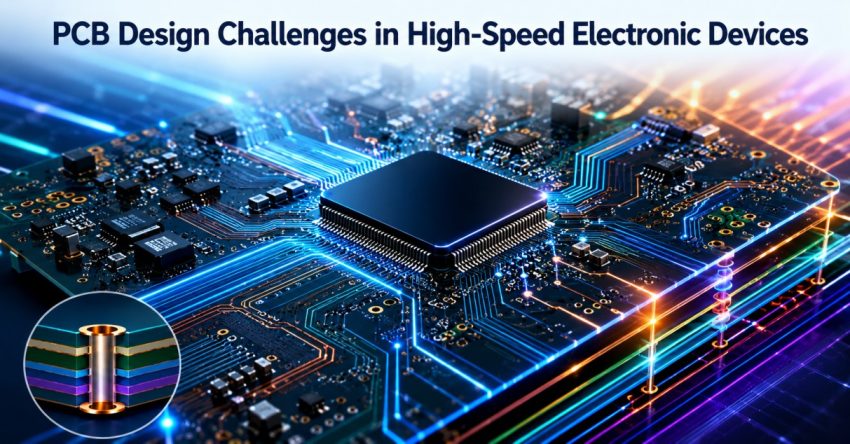
The need for faster, smaller and more powerful electronic devices has exploded in various industries including telecom, automotive, health, aerospace, and consumer electronic industries. As frequencies rise, complexity grows and engineers must plan and be precise. A well designed PCB is a key element to ensure that high-speed electronic devices operate without issues in terms of performance, safety and manufacturing.
Why High-Speed PCB Design Is More Challenging
The high speed electronic systems operate at frequencies at which layout imperfections will have an impact on the performance of the board compared to traditional circuitboards. Signal timing, electromagnetic interference and power integrity are all issues that need to be addressed during the PCB design process that become relevant.
The careful arrangement of components, optimization of trace routing, and selection of appropriate materials are crucial for engineers to ensure that signals are delivered efficiently, without distortion or delays.
Signal Integrity Issues
One of the biggest challenges in PCB design is maintaining signal integrity. Data rates become higher, electrical signals become more vulnerable to noise and adjacent trace crosstalk and reflections. These problems trigger issues in regards to miscommunication, poor system reliability, and device performance issues.
In order to tackle these challenges, engineers use controlled impedance routing, proper layer stack-ups, matched trace lengths, and differential pair routing. These techniques are used to ensure the signal does not become corrupted in the circuit board.
Power Distribution and Thermal Management
Today’s high-speed systems demand reliable power to all components, running concurrently. Frequent voltage fluctuations or too much electrical noise can cause a processor to perform poorly and can make a system unstable.
Use of dedicated power and ground planes, which can reduce voltage drops and enhance overall electrical characteristics, is an effective PCB design. Capacitors used to suppress unwanted noise and to provide stable power are called decoupling capacitors because they are positioned near ICs.
Another key factor to take into account is heat generation. Processors, graphics cards, and communications modules produce a lot of heat when running. The right placement of components, thermal vias, heat sinks and copper pours ensure that electronic components will not overheat and will serve for a longer period of time.
Electromagnetic Compatibility
Electromagnetic interference (EMI) is more difficult to control as electronic devices get smaller. If the boards are improperly designed, there may be interference with adjacent circuits or external equipment from unwanted emissions.
The ground rules outlined below are essential for creating a reliable PCB design that reduces electromagnetic interference: Ensure high-speed traces are not placed too close to one another; Practice proper grounding; Use effective shielding when required. Electromagnetic compatibility (EMC) standards are crucial to products that are intended for commercial or industrial use.
Manufacturing Considerations
There are a number of non-electrical requirements that must also be considered when designing a high speed circuit board. Another constraint is the ability of the engineers to manufacture the product and the assembly processes. Precision fabrication techniques are needed for extremely fine trace widths, close component spacing and multilayer board configurations.
Working closely with manufacturing teams in the design process can help minimize the risk of redesign and help maximize the quality of the product that is produced.
Conclusion
With electronic devices getting increasingly faster and more advanced, solving problems with fast circuit boards is more and more significant. All elements involved in the process of PCB design contribute to the effectiveness and efficiency of the finished product in terms of signal integrity, thermal management, electromagnetic compatibility, and many other factors.
Equipped with highly experienced and erudite engineers, Trident Techlabs provides the most advanced PCB design services suitable for modern-day electronic requirements. The knowledge, skills, and experience of the team along with the best industry practices and design software ensure the creation of reliable circuit boards that can perform complicated functions.
Also Read: How AI Is Changing the Future of Engineering Design